STX104 1.25V Differential Common-Mode Test Using Two Analog Outputs
The purpose of this test is to understand the common mode behavior of the STX104 +/-1.25V analog differential input range.
The analog outputs are wired back to the analog inputs using two female-to-female jumpers at J7 that are stripped off as a pair. The wiring is as follows:
- J7.16 DAC_OUT_2 → J7.35 CH0_LOW
- J7.17 DAC_OUT_1 → J7.36 CH0_HIGH
Analog output #2 (DAC_OUT_2) provides the baseline voltage to the analog input low side, while analog output #1 (DAC_OUT_1) sets the voltage to the analog input high side. In the software testing we fix the DAC_OUT_2 value and then vary the DAC_OUT_1 from below the negative input to above the negative input. The range of DAC_OUT_1 is set to be slightly beyond the +/-1.25V range.
The average of the two analog outputs is the common mode voltage.
Analog Common Mode Voltage = (Volts_DAC_OUT_1 + Volts_DAC_OUT_2) / 2.
For each setting of the two analog output channels we collect 8 analog samples, compute the average and record minimum and maximum values. Later in a spreadsheet we compute the standard deviation or RMS values.
We are able to provide a DC path for the analog input bias currents (even though they are extremely small, less than 10 nA) via the analog outputs. It is important to ensure that there is a DC return path back to analog common or ground so that these bias currents have a return path. If you are measuring a sensor with no ground return path, then one can add a 10K to 200K resistor from one of the differential inputs to ground. The companion STX104 40-pin terminal board has provisions to easily add these resistors.
The following STX104 jumpers are installed:
- Mode selection: M0, M1, M2, M4,
- Based address of 0x300: A9, A8,
- Analog output +/-5V range: DA1_UB, DA2_UB.
Note that the STX104 jumpers J8 and J9 are not installed.
Attached is source code to make this work. This is an Eclipse Project (including driver and applications). Code can still be compiled at the command line, see below.
aes-20211118223319.tar.gz updated November 18, 2021
To compile the code within Eclipse:
- Select and right click on aul_tree project and click on clean
- Select and right click on aul_tree project and click build. This will build the "libauldebug.a" library used by the demo program.
- Select and right click on "demo_stx104_range" project and click on clean.
- Select and right click on "demo_stx104_range" project and click on build.
To compile the code at the terminal:
- go to folder: aes_ws/aul_tree/_Out_Library_Static_Application_Debug. This will build the library that is used by the demo program.
- type: make clean
- type: make
- go to folder: aes_ws/demo_stx104_range/_Out_Debug
- type: make clean
- type: make
To compile the driver within Eclipse:
- Select and right click on drv_aul_x86 project and click on clean
- Select and right click on drv_aul_x86 project and click on build
To compile the driver at the terminal:
- go to folder: aes_ws/drv_aul_x86
- type: make clean
- type: make
To install the driver:
sh ./load_stx104
At the terminal, the program can be run as:
./demo_stx104_range --test:common
Test result spreadsheet: STX104_DIFFERENTIAL_1V25_GAIN_DAC_DRIVEN.ods (LibreOffice Calc file)
Note: The demo_stx104_simple project can be built and run in the same way as the demo_stx104_range demo program. This project provides a menu at the terminal and allows one to select and observe individual analog channels.
At the terminal go to folder aes_ws/_Out_Debug and type ./demo_stx104_simple to run it.
There is a documentation folder at aes_ws/documentation that contains additional information on all the projects and Eclipse setup.

Summary
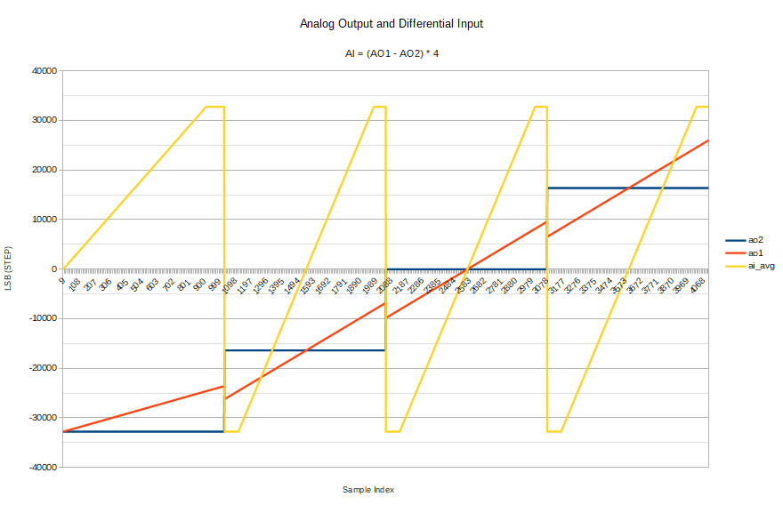
The plot below illustrates the behavior of the STX104 differential inputs at the +/-1.25V range. When the difference of the positive and negative input exceed +1.25V or -1.25V the output values rail.

The maximum number of steps or LSB that can be delivered is 32767 at +1.25V and -32768 at -1.25V; overall that is 16-bits of resolution. In some cases, sampling at a higher rate and performing a moving average or over-sampling can further improve resolution. You can see that as the differential input exceeds +1.25V or -1.25V, then the output value will rail at the maximum value and minimum value, respectively.
The overall RMS (standard deviation) value across all samples did not exceed 7 LSB. The average RMS value is typically less than 3 LSB. The peak-peak of the samples averaged about 7 LSB with a maximum value of 23 LSB; these large peak values are roughly from 86 out of 4096 (less than 2%) of the measurement sets. Some of the sampling error may have come from that our jumper wires were not twisted but a two wire ribbon; twisting may help to reduce the error. Further, the noise could also be coming from the analog outputs or other external sources.
Each step or LSB is approximately 38.15uV/step. This means that the typical RMS value is approximately 114uV and the typical peak-peak value is 267uV. We have not taken additional steps to reduce noise so there could be slight improvements (i.e. twisted wire jumpers, additional sampling and averaging).
We made an assumption the that gain and offset for each of the analog outputs are identical which they are not quite. But, the test does illustrate that the STX104 differential analog inputs will reject common mode easily and this test does not require any special equipment.
What we have demonstrated is that the 1.25V differential inputs to the STX104 behave as expected under a variety of common mode conditions.